Journey; All of this started when I bought a Dell Optiplex 7040 Micro to play around with different Linux Distros. When I opened up the mini PC, I saw two empty M.2 slots. One is a Key M slot and the other was a Key A slot. Those are for SSDs and WiFi/BT modules respectively. By this time, I was interested in making a custom PCB with high-speed signals with KiCad. When I saw those empty M.2 slots, an idea popped into my mind, “Why not make a custom M.2 PCB with PCIe signals”. In this article, I will elaborate the steps I took to make this happen.
Optiplex 7040M

The Dell OptiPlex 7040M is a pre-built business desktop computer. I has a lots of I/O and expandability.

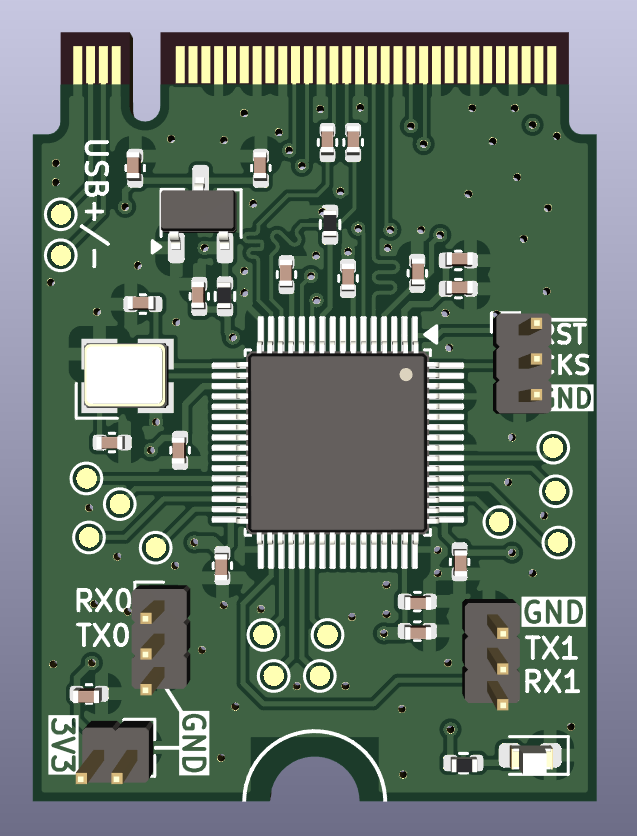
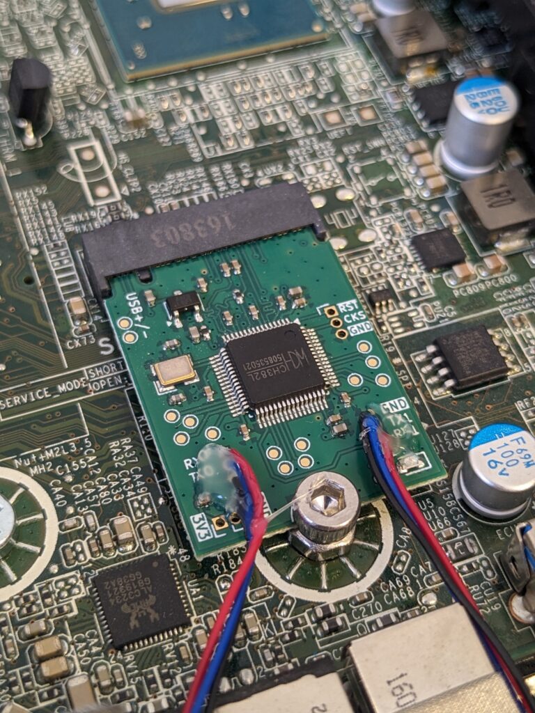
My primary focus was on the M.2 socket3 connector. I wanted to design a PCB that can use this socket and that can convert the PICe x1 interface to a UART COM port. The M.2 socket3 connector has a PICe 3.0 x1 interface. The physical format was 2230.
M.2 interface
M.2 interface comes in different electrical and mechanical formats.
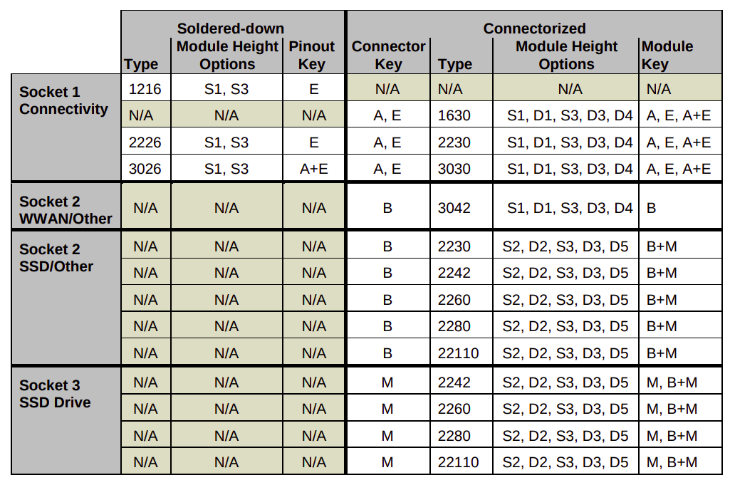
Socket 1 for connectivity (WiFI/Bluetooth), Socket 2 for WWAN/SSD/other and Socket 3 for SSD Drives. In my case, the mini PC had a Socket 1 with Key A.
Key A Electrical specification
- Power (3.3V, GND)
- WiFI-SDIO
- UART
- PCM (I2S)
- PCIe
- USB
- I2C
- Display Port
- Communication Specific signals
- NFC-UIM signals
PCIe signals
| Signal | I/O | Description | Voltage |
|---|---|---|---|
| PERp0, PERnp/ PETp0, PETn0 | I/O | PCIe TX/RX Differential signals defined by the PCIe 3.0 specification | |
| REFCLKp0/ REFCLKn0 | I | PCIe Reference Clock signals (100 MHz) defined by the PCIe 3.0 specification | |
| PERST0# | I | PE-Reset is a functional reset to the Add-In card as defined by the PCIe Mini CEM specification | 3.3V |
| CLKREQ0# | I/O | Clock Request is a reference clock request signal as defined by the PCIe Mini CEM specification; Also used by L1 PM Substates. | 3.3V |
| PEWAKE#/ OBFF | I/O | PCIe PME Wake. Open Drain with pull up on platform; Active Low | 3.3V |
PCIe to UART converter
After going through the JLC PCB parts list, I found the CH382 IC. It has PCIe x1, two UART and one Parallel port interfaces.

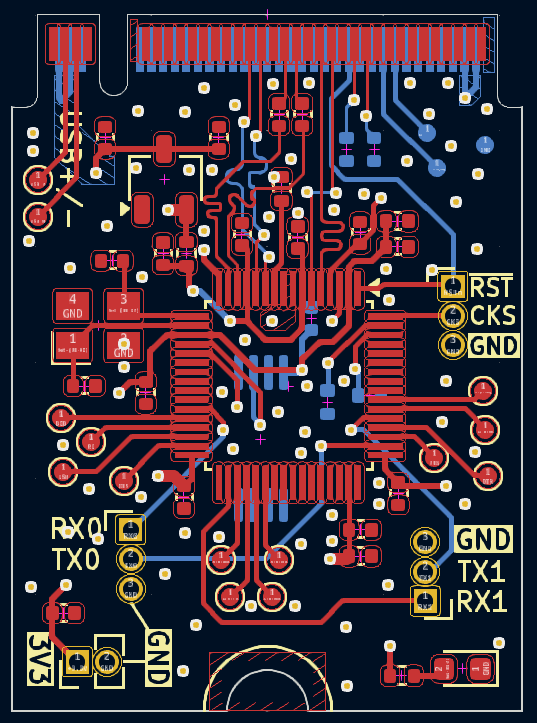
PCB Layout
PCIe impedance
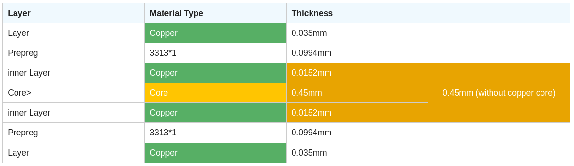
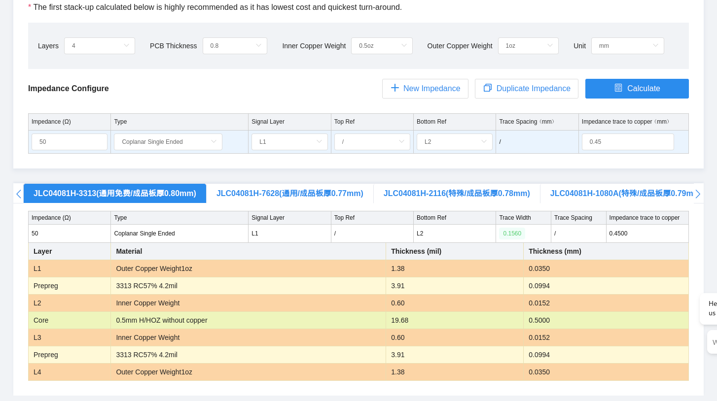
For the stack-up, I used the JLC PCB JLC04081H-3313 option. This provide me with 0.8 mm PCB thickness with 4 layers.
To obtain the 50 ohm trace impedance, I also used JLC PCBs impedance calculator, which gave me 156 um trace width.
With these information, I finished the layout in KiCad.
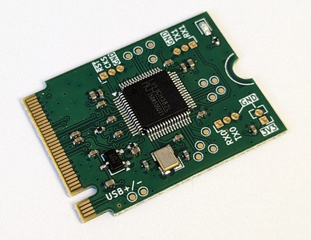
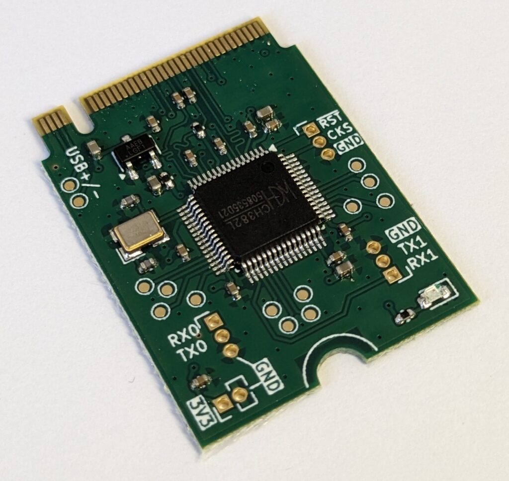
Production
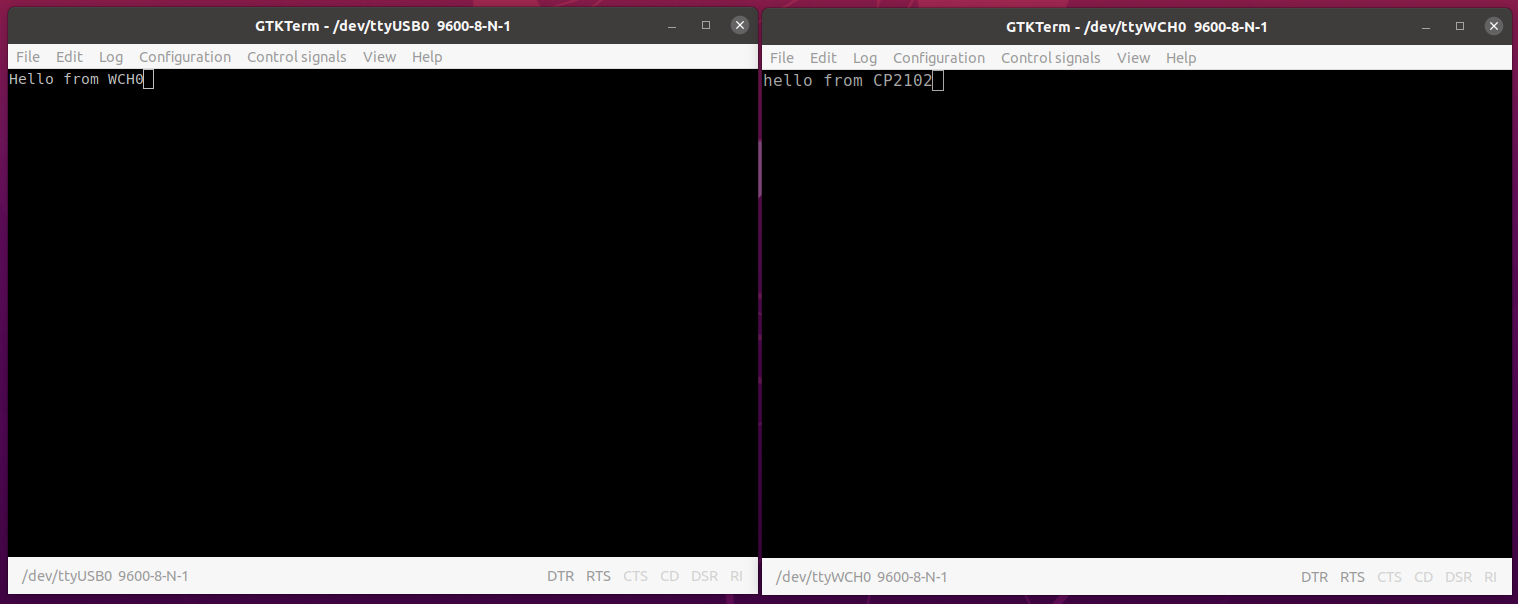
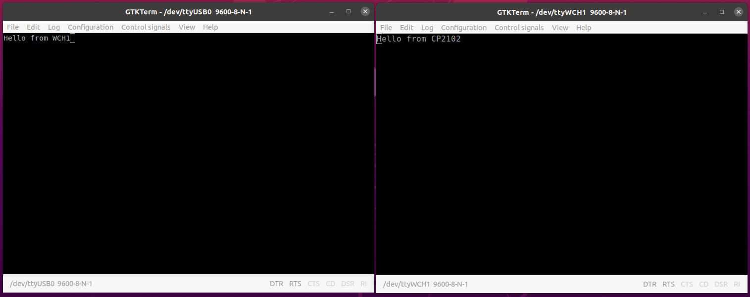
Installation & Testing
Windows
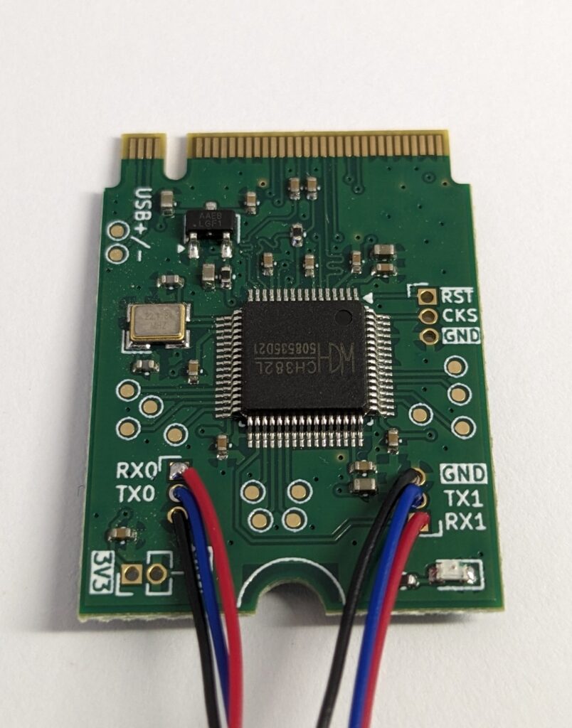
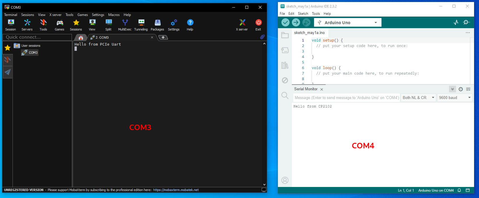
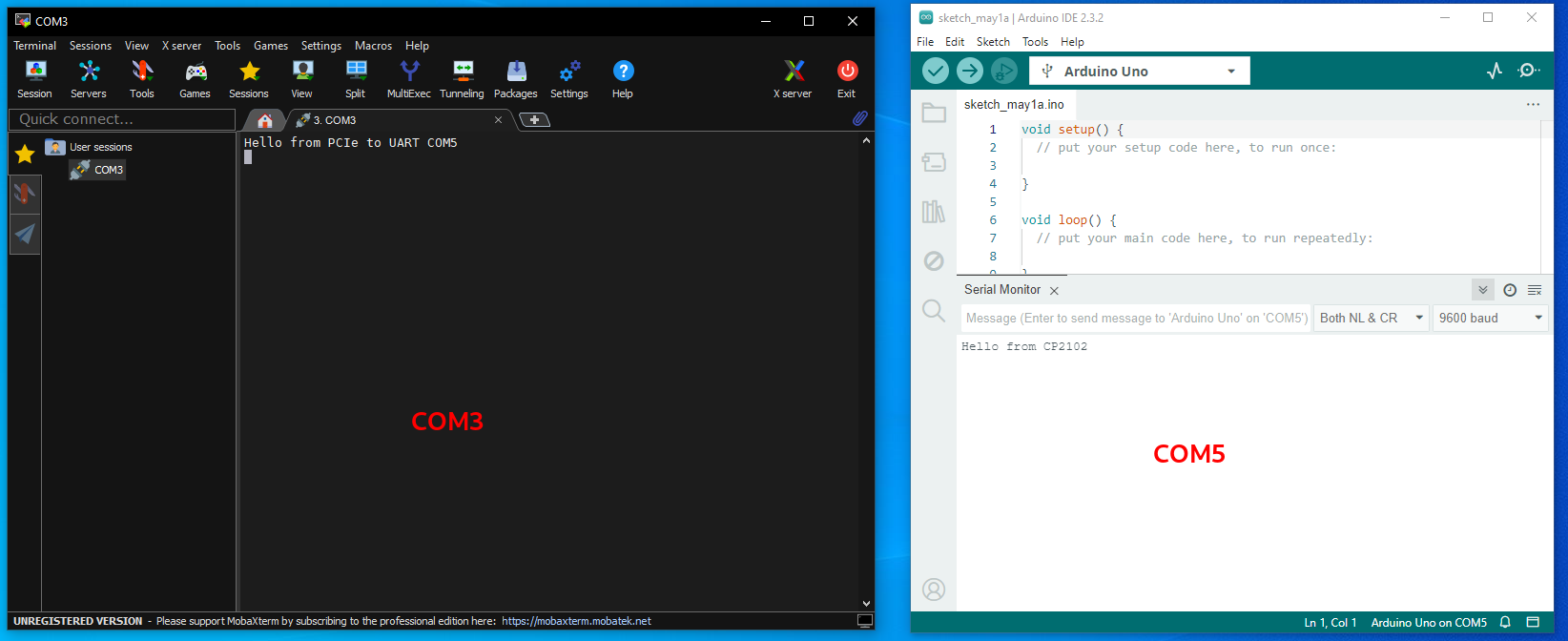
After installation, I installed the drivers provided by WCH. After that, two COM ports showed up in the device manager.

For testing purposes, I used another USB-to-UART converter, which showed up as COM3.
Ubuntu
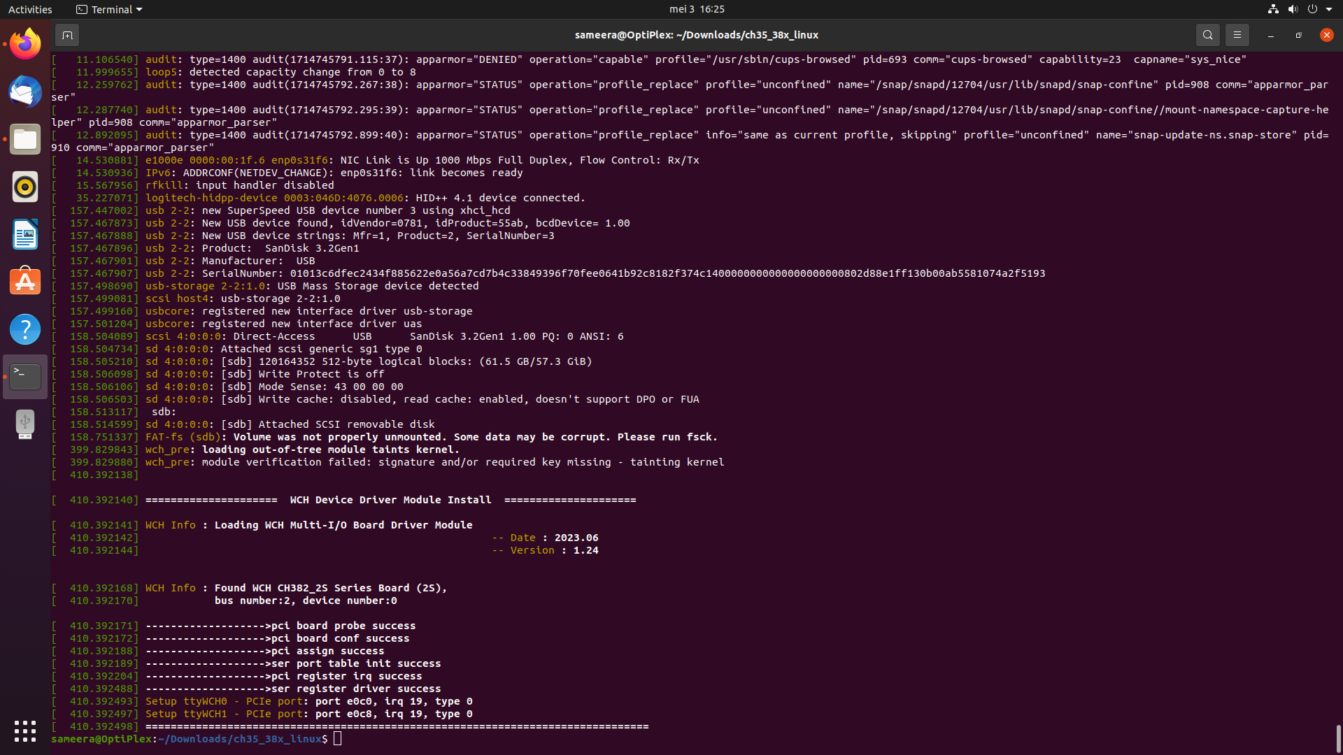
To use the module with Ubuntu, we need to compile the driver, which was taken from the Official Github link.
I was not able to build the driver with Ubuntu 22 (kernel 6.5). I was only able to do it with Ubuntu 20 (kernel 5.15).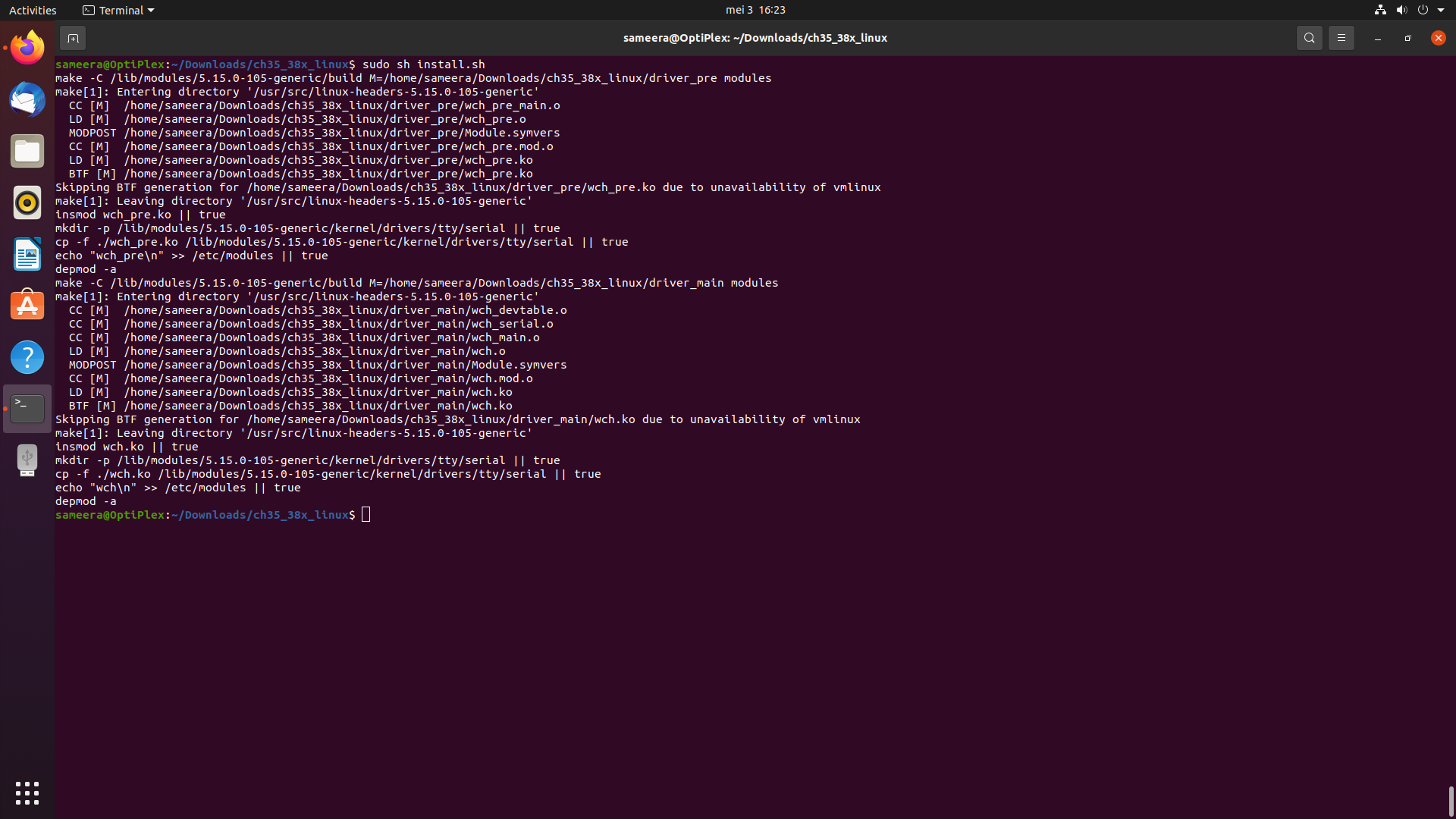
Conclusion
This project allowed me to get started with PCIe signal routing and it was a success. More projects with PCIe will come in the future.